Electronics are an integral part of our daily lives. Everything from our smart phones to our cars includes electronic components. At the heart of these electronics is the printed circuit board, also known as a PCB. Most people recognize printed circuit boards when they see them. These are the small green chips covered in lines and copper parts you’ll find at the heart of gutted electronic devices. Made with fiberglass, copper lines and other metal parts, these boards are held together with epoxy and insulated with a solder mask. This solder mask is where that characteristic green color comes from.
- +91 96633 97673
- Email: nithyasaadhana10@gmail.com
Electronics Sub-Assembly and Advanced Electronics
Electronics Sub-Assembly and Advanced Electronics
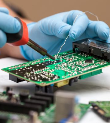
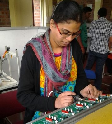
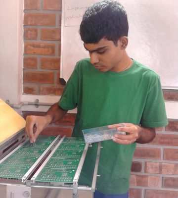
However, have you ever observed those boards with components solidly stuck on? Never regard them as just decorations of a PCB board. An advanced circuit board won’t be able to give its functionality until components are mounted on it. A PCB with components mounted on is called an assembled PCB and the manufacturing process is called PCB assembly. The copper lines on bare board, called traces, electrically link connectors and components to each other. They run signals between these features, allowing the circuit board to function in a specifically designed way. These functions range from the simple to the complex, and yet the size of PCBs can be smaller than a thumbnail.
There are two types of mounting technologies are prevailing in the modern PCBA industry
Surface Mount Technology: Sensitive components, some very small, such as resistors or diodes are placed automatically onto the surface of board. This is called SMD assembly, for surface mount device.
Thru-Hole Technology: works well on components with leads or wires that have to be mounted on board by plugging them through holes on board. The extra lead part has to be soldered on the other side of the board. This technology is applied on PCB assemblies containing large components such as capacitors, coils to be assembled.
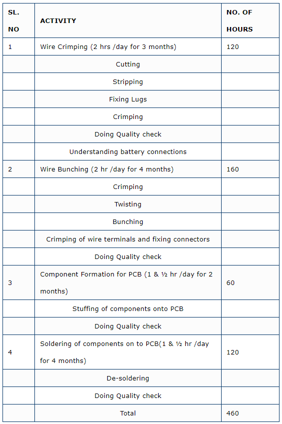
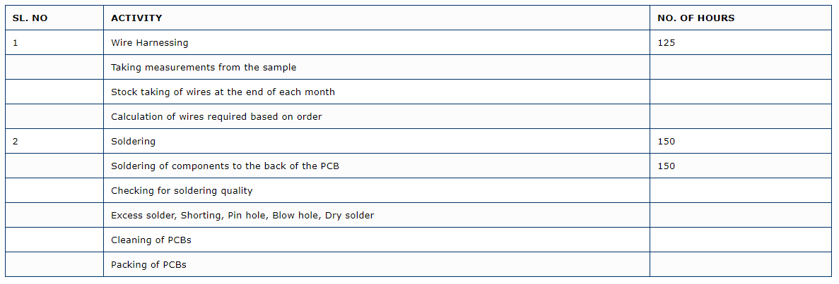
Thru-hole technology method of soldering is what the trainees learn at NITHYA SAADHANA
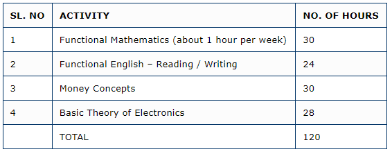
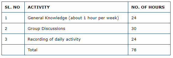
- This is the general guideline that can be followed for trainees with Intellectual Developmental Disorder
- The time taken to master a particular activity will definitely depend on the level of disability
- In Electronic sub assembly, all the areas of an activity may not be mastered by all trainees
- In functional and general behavioural issues, the expected gain in abilities will differ for each trainee depending on the severity of the disability


